

Silicon design complexity is ever-growing in resource demand. End users are demanding increasing levels of functionality, better battery life, and lower costs for all the different types of devices they use every day. This is driving chip makers to increase gate counts and push to ever-smaller silicon manufacturing modes. A good example of this rapid innovation is the expected production of 3nm nodes by 2022.
These requirements are creating exponential growth in all types of electronic design automation (EDA) workloads. Designers and their engineering IT colleagues are finding it challenging to keep up with demand. Adding thousands of servers to a data center can be expensive and time-consuming dynamically. In many cases, it may not even be practical to meet project budgets and schedules.
To keep up with the increasing demand on infrastructure, some organizations have started moving aggressively to the public cloud for EDA and more general high performance computing (HPC) workloads. The practically endless availability of central processing unit (CPU) and graphics processing unit (GPU) resources in the public cloud can allow designers to run large numbers of EDA jobs in parallel. Without being limited to on-premises data center resources, engineers can achieve a faster time to results with added business value of more simulations.
However, to achieve the optimal outcome, shared storage’s performance is a premium consideration. Under high parallelism compute, the data layer must be able to keep up with the very demanding concurrent workload by a large compute farm. This has been a major challenge for many semiconductor companies. A slow data layer will cause EDA jobs to wait, which then leads to longer runtimes and higher costs.
In addition, enabling EDA workloads in the cloud isn’t very straightforward. Among other issues, there are concerns around IP security, data governance, costs, and cloud lock-in.
Learn more in this video featuring Andy Chan, Director of Azure Global Solutions at Microsoft, and Ravi Poddar, Ph.D., Director of EDA/HPC Solutions at Pure Storage.
Connected Cloud Architecture for EDA Workloads
To address these challenges, Pure Storage, Microsoft Azure, and Equinix have joined forces to develop a connected cloud architecture for EDA, HPC, and other highly parallel workloads, such as software build and testing. The solution leverages Pure Storage FlashBlade®, the leading unified fast file and object (UFFO) platform. The all-flash storage platform delivers performance at scale.
In our architecture evaluation, we installed FlashBlade in an Equinix data center with a low-latency (under 2ms) ExpressRoute connection to an Azure region. We tested a variety of EDA and HPC workloads from Azure while using FlashBlade for data storage in Equinix.
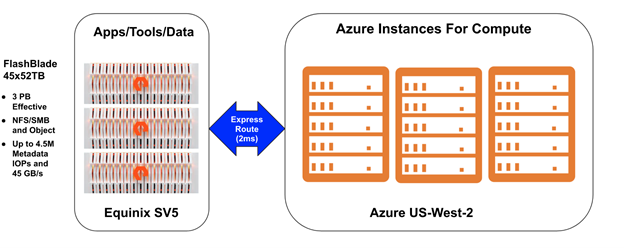
Figure 1: Architecture used to test the performance of FlashBlade in an Equinix data center with Azure.
This architecture offers several benefits:
- Security and Control: By storing your critical apps and data on Pure FlashBlade devices in an Equinix data center, you can reduce security/data governance, regulatory, and IP protection concerns. The Purity operating system provides best-in-class security and data management features. You’ll also have the ability to flex to multiple clouds without data migration.
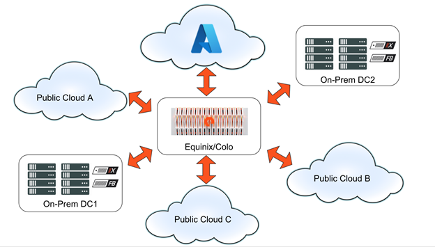
Figure 2: The connected-cloud architecture allows users to utilize multiple cloud providers and data centers without the need for data migrations.
- Simplified Cloud Adoption: Using array-level features, data can be staged and ready for cloud use at any time and in any location geographically. Scripts and flows can be adopted to cloud with minimal change.
- Performance at Scale: FlashBlade is a high-performance, all-flash storage system for file and object data. It can support hundreds of thousands of parallel TCP connections per chassis to enable high levels of parallel computation. FlashBlade provides:
- Support for up to 75GB/s and 7.5 million NFS metadata IOPS in one cluster
- Support for up to 9PB in one namespace with 2:1 (EDA data average) real-time data compression and encryption
- Linear performance scaling ability from 7 to 150 blades, non-disruptively
- Industry-leading performance on NFSv3, NFSv4.1, SMB, and object protocols to support a wide variety of workloads
- Cost Efficiency: With FlashBlade, simulations finish faster, thereby lowering instance usage. FlashBlade enables you to:
- Optimize EDA license costs and increase license usage efficiency
- Decrease storage usage with in-line data compression
- Reduce cloud egress costs by up to 70%
“Microsoft is thrilled to have worked with Pure Storage on the first-ever, connected-cloud solution for EDA workloads, giving customers more ways to use Azure to speed up semiconductor design flows. This cooperation demonstrates our commitment to providing customers with optimal storage options and enabling partners.” –Mujtaba Hamid, Head of Product, Modeling & Simulation, Microsoft Azure
“Expanding our relationships with Pure Storage and Azure to deliver this cloud adjacent storage solution is a clear win for customers — enabling them to more easily address the stringent performance, governance, and security requirements of HPC (high performance computing) and EDA (electronic design automation) for semiconductor workloads. Critical to this solution is a connected-cloud architecture that combines physical proximity and ultra-fast, low-latency, private connections between the Pure Storage FlashBlade and Microsoft Azure ExpressRoute infrastructure hosted at Equinix, unlocking a powerful new way for customers to push the high performance compute envelope.” – Zac Smith, Managing Director of Equinix Metal, Equinix
The connected-cloud architecture with FlashBlade and Azure is an excellent option for EDA and HPC workloads. The solution enables organizations to use the practically unlimited compute ability of the public cloud for next-generation product development while maintaining full control over data governance and security. This validated solution is the first of its kind for EDA/HPC workloads and can open up new opportunities and markets for your organization.
In particular, semiconductor design companies will be well-positioned to tackle sub-10nm projects. These projects can require up to four times more compute than they would need at larger geometries. They’re also critical for next-gen designs such as AI, 5G, IoT, mobile, autonomous vehicles, CPU, and GPU products.
Stay tuned for more posts in this series illustrating the performance of this architecture across various workloads. Our next post goes deeper into hybrid-cloud architecture for high performance computing workloads with Azure and FlashBlade.
Pure would like to thank the Azure EDA/HPC team for their unwavering collaboration and support for this solution development.
Giancarlo DiPasquale, Global Black Belt technical specialist Azure HPC
Jonathan Austin, Global Black Belt technical specialist Azure HPC
Damian Hasak, Director, Azure HPC+AI Solutions at Microsoft
Michael Requa, Ph.D., Program Manager, Azure HPC
Raymond Meng-Ru Tsai, Senior Program Manager, Azure HPC
Karl Rautenstrauch, Principal PM. Azure Storage Partners
Kevin Raines, Director Product Marketing – HPC at Microsoft
Andy Chan, Director, Azure Global Solutions, Semiconductor/EDA/CAE

![]()